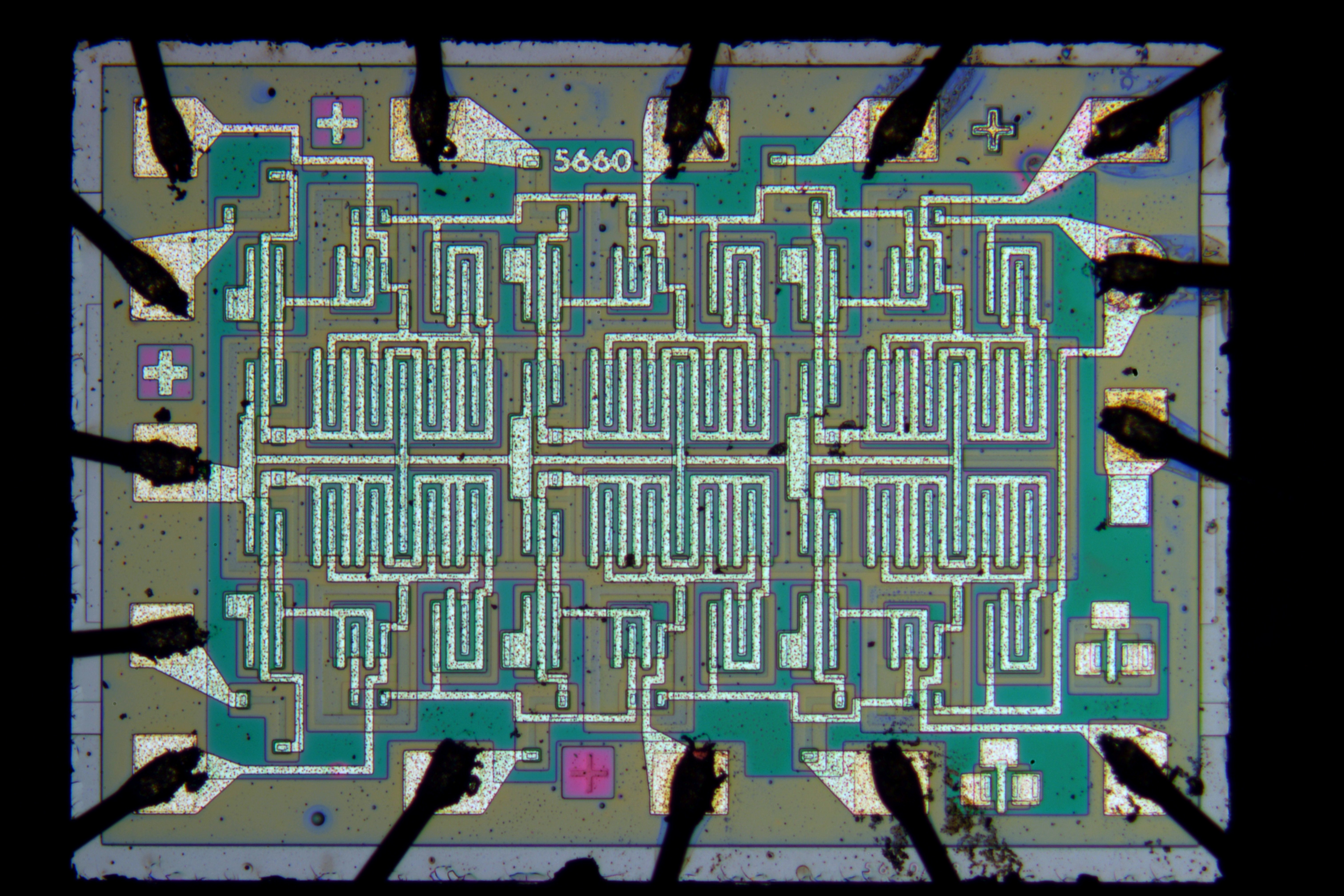
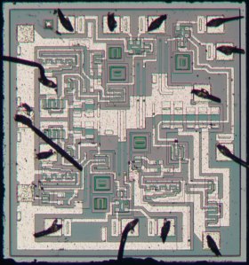
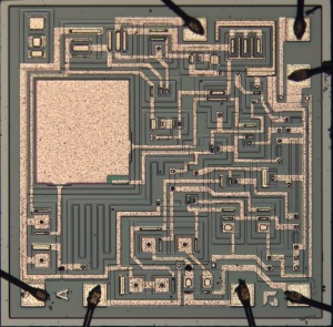
Lately, We have traced back the history of integrated circuits to a few very early devices, primarily manufactured by RCA and examples of ‘MOS’ type ICs. The metal-oxide-semiconductor geometry was the final design revolution, leading directly to modern chips. However, there were (and still are, unlike RCA) other manufacturers. Here’s a Raytheon RC1033 3-input NOR circuit:
The circuit logic is fairly easy to follow. Around the same time (1966), Motorola was producing the MC832P, a 4-input NAND gate:
later (1969!), Motorola was making the 3000L quad 2-input NAND gate:
and 3005L, a triple three-input NAND gate array:
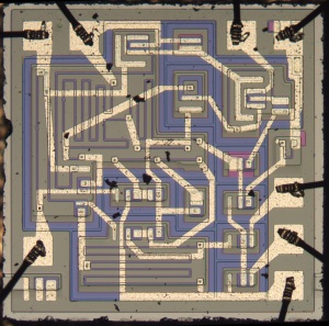
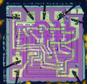
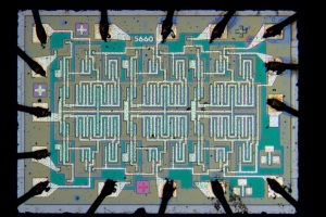
Yet another company, Fairchild Semiconductor, introduced a radically different kind of circuit- the operational amplifier. Here are images of the μA709, Fairchild’s breakthrough product:
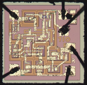
the LM710:
μA741:
and μA741 made by AMD the next year (1972):
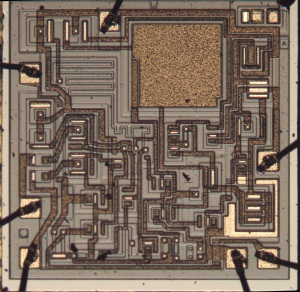
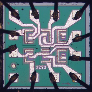
Lastly, here’s one we have yet to identify, part code U5B771239:
If you know what this is, let us know!
The Fairchild cicuits look radically different than the others- there’s no obvious symmetry to the layout, as opposed to the previous examples.
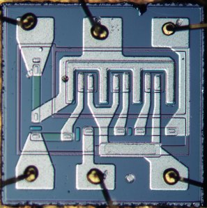
We opened up another RCA COSMOS chip: the 4007, a ‘dual complimentary pair and inverter’, which has a particularly simple layout:
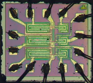
The layout is simply three pairs of transistors, p-type Field-effect transistors on the left, n-type FETS on the right. We know this because pin 1 is the round contact, and counting counter-clockwise, we identify pin 7 as the common voltage supply for the n-type transistors. On the circuit diagram, p- and n- type transistors are distinguished by the direction of the arrow located on the base terminal, and we also note that the transistors are enhancement mode devices.
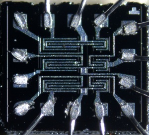
Now let’s consider a single transistor. These are field-effect transistors, which mean there are 4 terminals: source, gate, drain, and body/substrate. However, our images seem to have only three metal traces corresponding to source, gate, and drain: where’s the 4th terminal?
We can also see on the epi-illumination image that each transistor has 6 distinct layers: the ‘bottom’ layer where the bonding pads are, and then 4 intervening layers before the metal traces are reached on top. The oblique reflected light image does not show any other reflective metal, and the internal structure is only revealed by epi-illumination. However, one of those interior layers is a conductive layer that links pin 7 to the n-type transistors. A clue is given by the extra feature on the transistor immediately adjacent to pin 7; there is what appears to be a vertical conduction path to an interior layer, and this interior layer spans all three n-type transistors. So, it appears that we can identify the base/bottom layer, an insulating layer, and then a conductive layer followed by another insulating layer. The insulating layers are probably depletion regions.
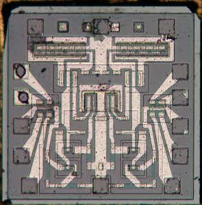
An even simpler design is the RCA 3018:
This IC has 4 transistors, two are isolated and the other two are connected in a Darlington configuration. A more complex IC is the RCA CD4009:
This IC consists of 6 inverters, and each inverter is constructed out of 5 transistors.
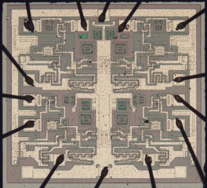
By now we have covered the early history of integrated circuits; these devices, or ones very similar, are the ones fabricated for the Apollo and Minuteman programs. However, so far we have only been looking at RCA chips; it could be interesting examine some examples from Fairchild, Motorola, and Texas Instruments to see what sorts of similarities and differences exist.